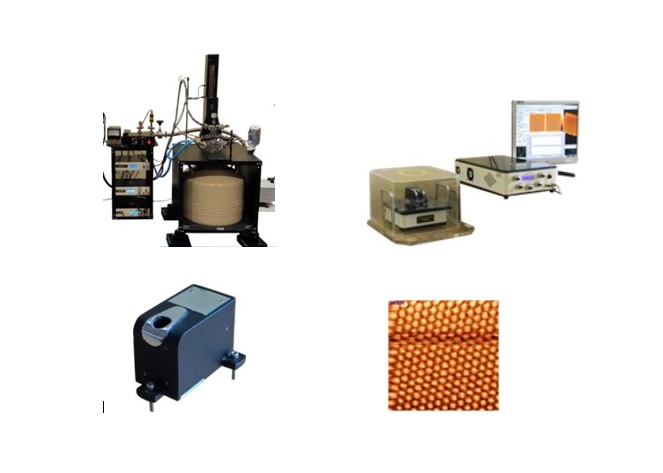
Scanning Tunneling Microscopy (STM)

Introduction
Scanning Tunneling Microscopy, commonly known as STM, is a powerful technique used to study the surface structure of materials at the atomic level. It was invented in 1981 by Gerd Binnig and Heinrich Rohrer, who later received the Nobel Prize in Physics for this discovery. STM allows scientists to view and analyze individual atoms on a material’s surface, making it an important tool in the fields of nanotechnology, materials science, and surface physics. It works only with conductive or semi-conductive surfaces and requires extremely clean and stable conditions to operate effectively.
Principle
The principle of STM is based on quantum tunneling. In this method, a sharp conductive tip is brought extremely close (within a nanometre) to the surface of a conducting or semiconducting sample. When a bias voltage is applied between the tip and the sample, electrons tunnel through the vacuum between them, creating a measurable tunnelling current. This current is highly sensitive to the tip-sample distance, allowing the instrument to detect atomic-scale features. By moving the tip across the surface and keeping the current constant, the microscope can map the surface’s structure with atomic resolution.
Application
Scanning Tunneling Microscopy is widely used in scientific research and industry. It helps scientists to observe and understand the arrangement of atoms on surfaces. STM combined with I–V curves provide local density of states (LDOS) at atomic sites.Helps in studying semiconductors, superconductors, and molecular. It is also used to detect surface defects, impurities, and changes in material composition. In advanced applications, STM can even be used to move individual atoms and build structures at the nanoscale, which is highly valuable in nanotechnology and materials engineering.
Completion of Installation
The installation of the Quazar Scanning Tunnelling Microscope (STM) instrument was successfully completed at the Central Laboratory for Instrumentation and Facilitation (CLIF), University of Kerala on 19th June 2025.
With the successful installation and training, the Quazar STM is now ready for routine operation and user facility support in surface and nanomaterial analysis.
Sample Requirements
For successful STM (Scanning Tunnelling Microscope) analysis, the sample must meet the following essential criteria:
- Conductivity : 0 to 10 mega ohms(conductive/semi conductive)
- Thickness : up to 0.5mm (0.7mm max)
- Size : within a 10mm diameter area
- Surface roughness: <100nm (very smooth)
- Sample preparation technique: Thermal/ RF sputtering/ Pulsed Laser Deposition (PLD)/Single crystal/Spin coating
- Substrate : Mount sample on a flat and rigid substrate like HOPG, Optical Drive, ITO glass.
Samples not meeting these conditions—such as highly insulating, rough, volatile, or poorly mounted specimens—may not yield reliable STM data.
